树莓派学习 — 初识GPIO
一 GPIO
GPIO全称是General Purpose Input Output (通用输入/输出)。广义上来说它并不是类似USB、DVI、HDMI这样一种特定协议的接口,而是通用接口的总称。对于了解单片机的人来说应该非常熟悉,而对于我们这些纯软件开发,没有接触过单片机的人来说,并不是很好弄清楚到底是个什么东西。 下面是维基百科的定义:
A general-purpose input/output (GPIO) is an uncommitted digital signal pin on an integrated circuit or electronic circuit board whose behavior—including whether it acts an input or output—is controllable by the user at run time.
从上面总结出几点:
- 数字针脚(可以是集成电路上的针脚,比如CPU或位处理器的针脚;也可以是开发板比如树莓派、Arduino上提供的GIPO接口)
- 可以用来输入或输出
- 运行时可控
二 树莓派GPIO功能
 树莓派提供了40个PIN口,大致的定义如下。其中黄色的GPIO PIN口有26个。 其余的是供电接口和接地口。每个GPIO接口都可以用作输入和输出,可以根据需要进行使用。
针脚电压
2个红色的针口提供了5V的输出电压,2个橘色的针口提供3.3V输出电压。 而8个黑色针口作为接地为0V。 其他的接口可以提供输入输出功能。所以
The 3.3 V rail can supply a maximum of 50 mA.
A maximum of 16mA per pin with the total current from all pins not exceeding 50mA.
输入/输出
对于GPIO接口来说,最重要的就是输入和输出功能。对于计算机来说能识别的只有0和1,而对于数字电路来说通过高低电平来表示输出的值是0还是1。
在买外设的时候发现,有些设备是5V高电平,有些是3.3V。了解到单片机分为3.3V和5V,就是指的是GPIO接口的电压。如果用GPIO口产生一个3.3V的高电平给一个5V的设备,可能会被认为是低电平,如果直接接上一个5V设备作为输入电平,可能会导致树莓派烧坏。所以使用外设是要注意这个外设的电压是5V还是3.3V。
当GPIO用做输入时,会有高电平、低电平、高阻态三个状态。
- 上拉电阻:电阻一端接VCC,一端接逻辑电平接入引脚(如单片机引脚)
- 下拉电阻:电阻一端接GND,一端接逻辑电平接入引脚(如单片机引脚)
A GPIO pin designated as an input pin can be read as high (3V3) or low (0V). This is made easier with the use of internal pull-up or pull-down resistors.
Pins GPIO2 and GPIO3 have fixed pull-up resistors ,but for other pins this can be configured in software.
更多上下拉电阻的概念可以参考:
- Pull-up and pull-down Resistors
- 上拉电阻与下拉电阻有什么作用
- GPIO电路图以及上拉电阻的作用
- 上拉电阻和下拉电阻
- 电阻(4)之上拉电阻与下拉电阻详解
GPIO数据传输
外设之间进行通信主要通过GOIP接口进行输入和输出。GPIO接口提供了可编程的方式从外设读取或向外设发送状态数据。通过控制控制高低电平可以输出不同状态,所以用做开关控制是非常简单有效的。作为输入时可以读取数值或者是状态。虽然每次只能传递0和1这样的数据,但是多次连续传递0和1组合起来,就可以传递复杂的数据。 比如温度传感器就是用GPIO口通过单总线协议进行数据交换。 通过GPIO可以进行各种协议的通信。
PWM
脉冲宽度调制(PWM),是英文“Pulse Width Modulation” 的缩写,简称脉宽调制,是利用微处理器的数字输出来对模拟电路进行控制的一种非常有效的技术。比如伺服电机使用输入PWM信号的脉冲宽度来确定它们的旋转角度,LCD显示器基于PWM信号的平均值来控制它们的亮度。PWM是根据频率和占空比进行震荡的数字信号(方波)
- 周期(Period):脉冲信号从一个上升沿到下一个上升沿的时间
- 频率(Frequency):描述1秒钟内脉冲周期发生的次数
- 占空比(Duty): 一个周期中高电平时间占整个周期时间的百分比

所以我们可以通过设置不同的占空比来控制脉冲宽度或者信号的平均值 ,从而达到控制外部设备的目的。下图是占空比为0,25%和100%。

PWM有硬件和软件两种输出方式:
- 软件方法:将普通GPIO引脚作为PWM输出引脚,依据实际需求,配置好计时器,在指定计时周期翻转GPIO引脚电平,实现PWM功能。通过终端方式实现,占用CPU,精度差,控制复杂
- 硬件方法:在原理图设计时,将支持硬件PWM的引脚作为PWM输出引脚,这样就可以直接通过配置寄存器,采用硬件实现PWM功能了。通过事件方式实现,不占用CPU。
PWM (pulse-width modulation)
- Software PWM available on all pins
- Hardware PWM available on GPIO12, GPIO13, GPIO18, GPIO19
I2C
I2C (Inter-Integrated Circuit)是一种简单、双向二线制同步串行总线。它只需要两根线即可在连接于总线上的器件之间传送信息。主要用来和一些简单的外设进行小数据的传输。一般连接一些传感器或驱动器,比如速度传感器、温度传感器、LCD显示器或电动马达。
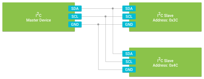
- Shared clock signal (SCL): 因为I2C是串行的,所以需要SCL时钟总线发出信号来同步主从设备间的数据传输,发出时钟信号的设备为Master,而连接的设备为Slave。
- Shared data line (SDA):主从设备间通过SDA总线进行数据传输,
因为只有一根数据线,所以I2C接口是半双工。 - Common ground reference (GND) : 接地
I2C接口支持多个设备连接在同一个总线上。每个设备都有自己的地址,但是这个地址是软件实现的,这个地址用7bit表示,所以理论上I2C最多可以连接128个设备。而因为通信协议中带上了设备地址, 所以同时只能和一个设备通信,设备只会响应传递给自己地址的数据。I2C接口传输速率有Master的时钟频率决定。树莓派上默认是100KHZ。这个需要根据外设来进行设置。
I2C
- Data: (GPIO2); Clock (GPIO3)
- EEPROM Data: (GPIO0); EEPROM Clock (GPIO1)
SPI
SPI是串行外设接口(Serial Peripheral Interface)的缩写。是一种高速的,全双工,同步的通信总线。SPI有比较高的传输速度,所以适合用看来进行带宽要求比较高的数据传输,比如图像的传输。很多传感器都支持SPI和I2C接口。
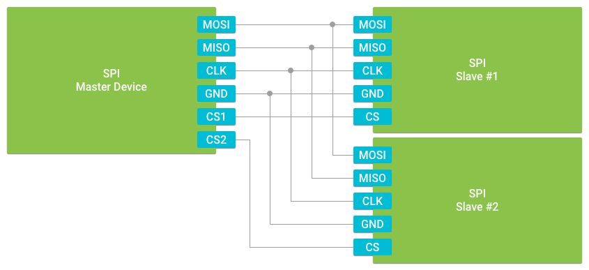
- Master Out Slave In (MOSI) 数据总线,用于master向slave发送数据
- Master In Slave Out (MISO) 数据总线,用于master接收slave发来的数据
- Shared clock signal (CLK) 时钟总线,因为SPI是一个同步接口,所以也需要时钟总线来同步传输
- Common ground reference (GND) 接地
- CS 片选信号线,如果只有一个设备不需要
因为
SPI
- SPI0: MOSI (GPIO10); MISO (GPIO9); SCLK (GPIO11); CE0 (GPIO8), CE1 (GPIO7)
- SPI1: MOSI (GPIO20); MISO (GPIO19); SCLK (GPIO21); CE0 (GPIO18); CE1 (GPIO17); CE2 (GPIO16)
UART
通用异步收发传输器(Universal Asynchronous Receiver Transmitter), 一般也简称为串口(serial ports)。我们在使用电脑时也经常通说串口,比如老的COM口、现在的USB口。所以大家说串口一般是一个总称,而单片机上一般书串口指的是UART,它使用TTL电平(2.6V-5V为1,0为0-0.4V),而电脑上的COM口使用RS232电平 (逻辑1=-3V~-15V逻辑0=+3~+15V) 。
串口、COM口、TTL、RS–232、RS–485区别详解

UART接口是异步接口,所以不需要时钟总线。设备之间的传输速率是可以协商的,所以是通用接口。 设备直接通过RX和TX两个数据总线连接,所以是全双工模式。UART接收到的数据会放到一个FIFO队列中,直到设备读取。UART支持3线和5线两种连接方式:
- 3-Wire ports include data receive (RX), data transmit (TX), and ground reference (GND) signals.
- 5-Wire ports add request to send (RTS) and clear to send (CTS) signals used for hardware flow control. Flow control allows the receiving device to indicate that its FIFO buffer is temporarily full and the transmitting device should wait before sending any more data.

5线相比3线多了RTS和CTS两条控制总线。作用就是当FIFO队列满了的时候通知设备暂时不要传递数据。和I2C以及SPI不同的是,UART是点对点通信。速度比I2C块,但是可能要比SPI慢。
Serial
- TX (GPIO14); RX (GPIO15)
小结
之前对GPIO的理解有点偏差,认为普通GPIO口只能发送0,1作为开关,而其他I2C,SPI等接口可以发送负责的数据。 后来发现一些外设就是通过普通GPIO口来进行了单总线通信。 所以GPIO确实只能产生高低电平,但是如果连续产生,就可以连续的发送数据给设备。 而I2C, SPI这些总线本质也都是发送电平,不同的是他们是按指定的协议方式发送。 而实际外设中有很多是自定义协议,所以理论上无论是自定义协议,还是标准的I2C,SPI这些协议,都是可以用任意的GPIO口来通信的。
只是PI上定义了I2C, SPI这样的接口,如果不使用这些接口,而用普通GPIO接口就需要自己来实现这个协议,而不能使用已有的I2C,SPI的库来通信。对于自定义协议也是一样。其实设备的针脚是可以任意GPIO的、只是如果使用了已有的库文件,需要修改对应的针脚设置。所以GPIO功能是非常强大的,你可以使用GPIO来和任意协议的设备通信,可以用GPIO来模拟USB通信,设置你可以模拟硬盘IDE接口和硬盘通信。当然在速度上可能会有
三 GPIO编程
前面都是一些和硬件相关的基本支持,对于码农来说的主要还是通过编程来实现各种设备的共功能。和硬件交互我们听到最多的就是驱动程序。下面是维基百科对设备驱动解释:
In computing, a device driver is a computer program that operates or controls a particular type of device that is attached to a computer.[1] A driver provides a software interface to hardware devices, enabling operating systems and other computer programs to access hardware functions without needing to know precise details about the hardware being used.
A driver communicates with the device through the computer bus or communications subsystem to which the hardware connects. When a calling program invokes a routine in the driver, the driver issues commands to the device. Once the device sends data back to the driver, the driver may invoke routines in the original calling program. Drivers are hardware dependent and operating-system-specific. They usually provide the interrupt handling required for any necessary asynchronous time-dependent hardware interface.[2]
原文
GPIO电路图以及上拉电阻的作用
GPIO口的定义
GPIO口,通用输入输出,这个大家都知道,但是输入,输出的电路是什么样的,其实并不用太关心,只需配置寄存器即可,但是还是要摸一摸,为了方便理解,引入了单片机的IO口原理图来说明(道理是一样的)
认识电路
一.普通IO口
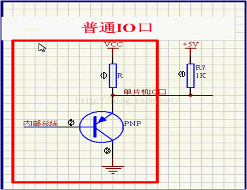
如上图所示(红色框是板子内部)
1.基级(②位置)为低电平时,PNP导通,此时单片机IO口输出的是低电平,当基级(②位置)为高电平时,PNP导通,此时单片机IO口输出的是高电平
2.这里注意,④位置上是一个上拉电阻,这里设置上拉电阻的考虑因素是这样的,假设我要在这个单片机IO口输出一个电流来驱动小灯发亮,①的位置电阻一般有20k左右,发出的电流250uA,基本上忽略不计,加上一个上拉电阻后, 总电流 = ①位置电流 + ④位置电流(①与④构成并联电路)
3.为什么不设置让,①的位置电阻R小一点,这样电流大一点,就不需要上拉电阻了呢? 因为单片机是控制单元,设计时最好把强电流设计到外围电路里,如果设计到单片机内部,会烧坏板子
这里体现出上拉电阻的其中一个作用—>加大电流,加强了驱动的能力
二.强推挽输出
(意思就是说能输入输出大电流,前面已经说了单片机内部最好不要设计大的电流,所以这个功能的IO要少用)
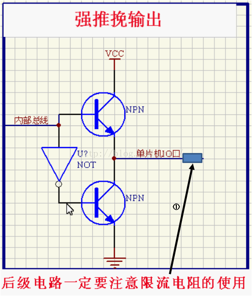
- 内部总线输入高电平, 上面的NPN导通,则IO口输出大电流(因为上面的三极管VCC电源下面没有接上拉电阻, I = VCC/电阻+NPN内部电阻),所以IO出口的地方一般接一个电阻限流内部总线输如低电平, 下面的NPN导通,则此时如果IO口外面接一个VCC(不带上拉电阻),就会有大电流灌输进来
这里体现了上拉电阻的另一个作用—>限流
三.开漏级OC门
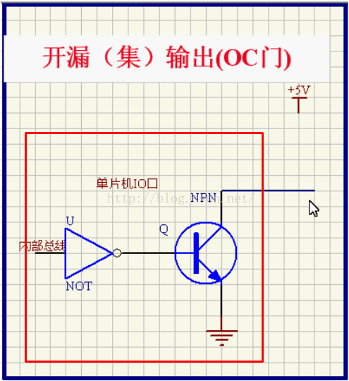
什么叫IO口的开漏状态,如上图所示 如果内线是高电平,则NPN的基级是低电平,此时NPN不导通,那么IO口此时相当于是悬浮在空气中的,所以无法确定它的状态(不知道是低电平还是高电平),那么这个状态就是开漏状态,所以此时要向外围电路输出一个高电平是不可能的,如果想输出一个高电平,则必须在NPN的集电极上面来一个上拉电阻
这时又体现出上拉的一个作用:
这里对于OC门还有一个应用, 可以控制高电位的电路,如果外围电路需要大的电压,则可以用OC门加上拉电阻来完成这个功能,如下图所示, 当内部总线为高电平,则NPN截止,最右边加一个12v的上拉电阻,使得电位钳在12v供外围电路使用
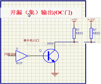
上(下)拉电阻详细说明
上拉电阻、下拉电阻一般是给一个电平不确定的信号确定一个电平。
上拉就是输入高电平,然后接一个上拉电阻(起保护作用),将不确定的信号通过一个电阻钳位在高电平,电阻同时起限流作用。
下拉就相反了,指输入低电平,然后接一个下拉电阻,将不确定的信号通过一个电阻钳位在低电平。
不过从程序设计的角度讲,上拉就是如果没有输入信号则此时I/O状态为1,下拉则是无信号输入时I/O状态为0。
具体配置为上拉还是下拉,要看电路图。看外部有没有上下拉电阻。
上拉电阻有时是用来解决总线驱动能力不足时提供电流的,一般说法是拉电流;下拉电阻是用来吸收电流的,也就是灌电流。比如有I2C总线使用会上拉一个10k的电阻。
端口选择还应该注意端口的初始的状态。这个状态是系统复位时的状态,是不受上层软件控制的,假如选择的端口正常是高电平有效的,那么应该选一个系统复位时,是下拉状态的端口。
上拉电阻
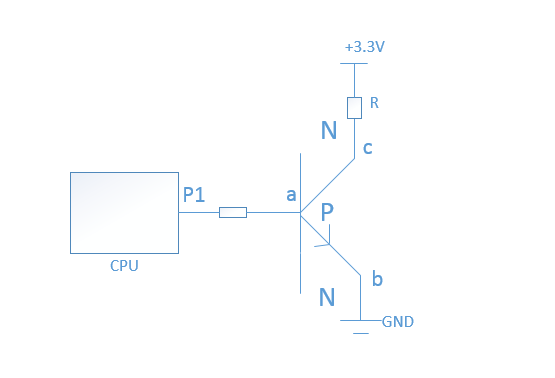
P1管脚为输出,R接+3.3V为上拉电阻,三极管为NPN型。
若单片机输出为低电平,则a、b不导通,导致c、b不可导通。如果没有上拉电阻R,则c处悬空,电平无法得知。接上上拉电阻,由于上拉电阻接3.3V,可得c处电平为高。
若单片机输出为高电平,则a、b导通,导致c、b可导通。如果没有上拉电阻R,则c处悬空,电平无法得知,也无法知道c、b是否导通。接上上拉电阻,由于上拉电阻接3.3V,c直通b,得c为低电平。
下拉电阻
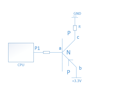
P1管脚为输入,R接地为下拉电阻,三极管为PNP型。
若单片机输出为低电平,则a、b导通,导致c、b可导通。如果没有下拉电阻R,则c处悬空,电平无法得知。接上下拉电阻,bc导通,c接3.3V为高电平。
若单片机输出为高电平,则a、b不导通,导致c、b不可导通。如果没有下拉电阻R,则c处悬空,电平无法得知,也无法知道c、b是否导通。接上下拉电阻,由于下拉电阻接地,得c为低电平。
拉电流负载和灌电流负载
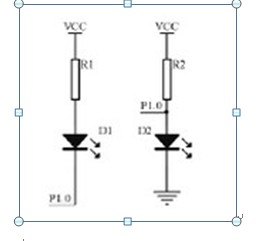
图左是灌电流负载。单片机输出低电平时,LED亮,;输出高电平的时候,那就什么电流都没有,此时就不产生额外的耗电。
图右是拉电流负载。单片机输出低电平的时候,LED不亮,此时VCC通过R2把电流全部灌进单片机IO口,并且电流时5ma。
单片机输出高电平的时候,VCC通过R2将电流注入到LED中,led亮(说法不对,应该是P1.0引脚的电压Vcc直接通过发光二极管将特大电流注入二极管)。注意到了吗? LED 不发光的时候,上拉电阻给的电流全部灌入单片机的引脚。如果在一个 8 位的接口,安装了 8 个 1K 的上拉电阻,当单片机都输出低电平的时候,就有 40mA 的电流灌入这个 8 位的接口。如果四个 8 位接口,都加上 1K 的上拉电阻,最大有可能出现 32 × 5 = 160mA 的电流,都流入到单片机中。这个数值已经超过了单片机手册上给出的上限。此时单片机就会出现工作不稳定的现象。而且这些电流,都是在负载处于无效的状态下出现的,它们都是完全没有用处的电流,只是产生发热、耗电大、电池消耗快…等。
答:这也不行,因为需要它为拉电流负载提供电流。对于 LED,如果加大电阻,将使电流过小,发光暗淡,就失去发光二极管的作用了。在图右,假如单片机输出的高电平时3V,此时R2两端的电压差为5V-3V=2V。经过R2的电流为I=2V/1000=2ma,这一部分电流将全部流入LED。如果加大电阻,上拉电阻提供的电流将会减小。
GPIO of Raspberry PI
Introduction
In reading about using the GPIO pins of either a Raspberry Pi, an Arduino, or some other single-board computer or micro-controller, you have probably seen reference to pull-up and pull-down resistors. But what are they and why do we need them?
Before explaining their use, we need to understand the nature of a general-purpose input/output pin (GPIO pin).
Logic Levels and GPIO Pin States
The purpose of a GPIO pin is to either influence the action of an external circuit, by toggling the high or low state of the pin used as an output, or to monitor the state of some external circuit on a pin configured as an input.
But what do we mean by high or low?
The general-purpose input/output pins on the Raspberry Pi
In reality there will be a level somewhere between zero volts and 3.3 which represents the threshold above and below which the state is said to be either low (below the threshold) or high (above the threshold).
Let’s assume this threshold is 1.65 volts, half-way between zero and 3.3 volts.
Now let’s assume we have configured one of the pins as an input, to monitor the state of a momentary press button. That is, a button which does not latch, but which has contacts which are closed when it is pressed and open when it is not.
How should we wire this button to the pin, so that when it is pressed, the state of the pin is low, and when it is not pressed, it is high.
The answer is to wire the button so that it forms one part of a potential divider with either a pull-up or a pull-down resistor.
A Potential Divider
What is a potential divider?
Two or more resistances in series across a potential difference, a voltage, form a potential divider, because they divide the potential.
Imagine two resistances of exactly equal resistance, wired in series across a voltage (V).
Imagine that one end of that divider is connected to ten volts, and the lower end is connected to ground, or zero volts.
Measured at the mid-point, the junction between the two resistors, the value measured will be half of the full potential, or 5 volts.
Resistor and Button as Potential Divider
We need a circuit that makes quite sure that when we want the GPIO pin to register as being in the high state, in other words to measure high when the button is not pressed, and to register low when it is, we need to make quite sure the voltages at the GPIO pin are either well below the threshold level (in the low state) or well above it in the high state.
If the level at the GPIO pin is allowed to float or hover at or close to the threshold level we will get false results.
The circuit
There needs to be a connection between 3.3 volts, with reference to the Pi supply, and the GPIO pin, and the button needs to be wired between the pin and ground.
But why do we need a resistor? Can’t we just connect the 3.3 volt supply directly to the GPIO pin?
Short Circuit
The term short circuit, I’ve always thought, is a bit of a misnomer, because it isn’t always particularly short.
It refers to a situation in which excessive current can flow because a very low resistance, typically just a conducting piece of wire, is accidentally connected between a point of high potential, such as the supply rail, and a point of much lower potential, like ground.
If this is allowed to happen, damage can result to components in the circuit, and possibly to the whole assembly because of excessive current flow and the resulting generation of heat.
Limiting Current Flow
So, we need to connect the GPIO pin to 3.3 volts via a resistor so that current is limited.
Refer to [the page about Ohm’s Law elsewhere on this site][ohms] for details of how this works.
The whole circuit
The resistor and the button now form a potential divider.
But, when the button is not pressed, the resistance across it is so high it can be thought of as being open circuit, in fact it is open circuit. If we used a very, very high number of Ohms to represent the open button, and used, for example a 4.7 kilohm resistor, we could calculate that the voltage at the GPIO pin will be as close to 3.3 volts as makes no difference.
But when we press the button, the contacts of it are now so low in resistance, that the situation is reversed, and the 4.7 kilohm resistor is now much, much higher in resistance than the closed contacts of the button.
And here we see the reason for the resistor as opposed to just a piece of wire.
Remember:
If V is 3.3 and R is 4.7 kilohms then:
I = 3.3 / 4.7
Or a number which is low enough to not cause any damage to the supply, or to generate any significant heat in the circuit. In fact it is below 1 milliamp. Remember from the [Ohm’s Law][ohms] page that if we use a value of kilohms in the calculation, our answer will be in milliamps.
And because the contacts of the button are so low in resistance as to be considered as a short to ground, the voltage measured at the GPIO pin will be almost zero, and well below the threshold.
The above is an example of using a pull-up resistor to make sure that when the button is not pressed the GPIO pin is pulled up close to the 3.3 volt level and well above the threshold, preventing any intermittent state-change events caused by the voltage hovering at or around the threshold.
Pull-down
If we wanted to reverse the situation, to make the GPIO pin register a high state when the button is pressed and a low state when it is not,
In this configuration the resistor is again there to limit the flow of current when the button is closed, and because, when the button contacts are open, the resistance it presents is much, much higher than the 4.7 Kilohm resistor, the level measured at the GPIO pin is as near to zero as makes no difference. Hence the resistor is pulling the level down to, or close to ground potential and making sure the pin does not hover around the threshold.
Switch Contact Bounce
There is a complication which, although it is not directly concerned with the subject of this page, is worth mentioning here.
That is the tendency of the contacts of a switch or the contacts of a relay to bounce when they close.
Imagine the button contacts to be two small flat plates of copper which come together when the button is pressed.
If you could record the closure of the contacts at a very high frame-rate and play it back in slow-motion and much magnified, you would observe the contacts bouncing as they come together.
This does not matter at speeds at which humans operate, but at the clock-speed of the CPU in a computer or micro-controller, the result would be a brief but disturbing moment of the high to low state change being repeated several, or even many times.
For this reason electronic circuits typically employ extra components to electronically dampen this bounce and eradicate it’s effects.
The GPIO libraries used in the Raspberry Pi and in the Arduino provide a mechanism for inserting a delay when a state-change is detected to give the contacts chance to stop bouncing, and prevent repeated events from being triggered. Typically this delay is just several milliseconds.
Internal pull-up and pull-down Resistors
Some micro-controlelrs include internal pull-up or pull-down resistors, and this is true in the case of the Raspberry Pi.
The GPIO libraries provide for configuring code to either use these internal resistors or to emply external ones.
Edge-triggering
If you could see the state of the junction at the GPIO pin graphed on the screen of an oscilloscope, the change from low-to-high or the change from high-to-low would look like a very rapid rise or fall of the level.
This is called the edge, and it is this which the GPIO libraries used in micro-controllers and that used in the Raspberry Pi typically look for.
If the contacts of our button were not de-bounced, either by adding a delay when the first edge is detected, or by adding other electronic components which clean up this change of state, we would see on the screen what looks like several teeth of a comb as the state rapidly changes from one to the other.
引用
ccarea.cn
csdn
csdn
raspberrypi